
The Conductivity Spectrum: Understanding the difference between Antistatic, ESD, and EMI Shielding (10² vs 10⁹ Ω)
Understanding the difference between Antistatic, ESD, and EMI Shielding is critical for industrial engineers selecting conductive polymers. Selecting the correct material is a function of specific Volume Resistivity or Surface Resistance requirements.
However, using an EMI-grade material for a simple antistatic tray is overkill. Conversely, using an antistatic material for shielding will result in immediate component failure. Below is the technical breakdown of the Antistatic, ESD, and EMI Shielding spectrum.
| Category | Range (Ω) | Primary Application |
|---|---|---|
| Antistatic | 109 – 1012 | Dust Prevention, Packaging |
| ESD / Dissipative | 106 – 109 | Circuit Board Assembly, Jigs |
| EMI Shielding | 102 – 105 | Avionics, Housings, Defense |
Defining the Antistatic, ESD, and EMI Shielding Ranges
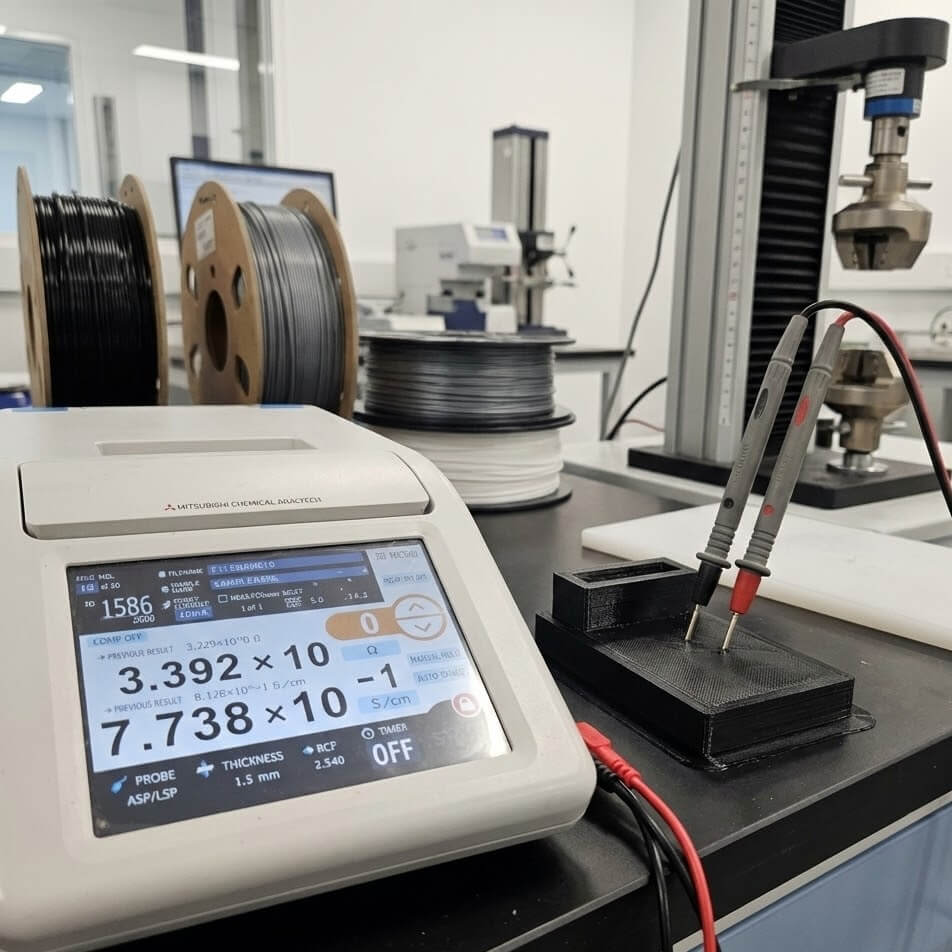
At ABC3D, we classify our materials into three distinct electrical ranges based on ohms per square (Ω/sq) or ohm-cm. Because we are a vertically integrated manufacturer, we can tune our masterbatches to hit these specific targets.
1. Antistatic (109 to 1012 Ω)
Antistatic materials effectively prevent the buildup of static electricity. However, they have high resistance, meaning the charge moves very slowly across the surface.
- Primary Function: To suppress initial triboelectric charging (friction-induced static).
- Typical Application: Electronic packaging, dust covers, and safe-handling trays.
- ABC3D Solution: Our standard ESD-Safe PETG often falls into this versatile range.
2. Static Dissipative / ESD (106 to 109 Ω)
This is the “Sweet Spot” for electronics manufacturing. Static Dissipative materials allow charges to flow to ground, but they do so at a controlled rate. Consequently, this prevents the “spark” or rapid discharge that destroys sensitive circuit boards.
- Primary Function: Controlled removal of charge to ground.
- Typical Application: Assembly jigs, circuit board housings, and pick-and-place nozzles.
- Why it matters: If a material is too conductive, it can short out the board. If it is too insulative, it holds the charge. ESD grade is the perfect balance.
3. Conductive / EMI Shielding (102 to 105 Ω)
Finally, we have the highly conductive range. These materials have low resistance, allowing electrons to move freely. Furthermore, this level of conductivity is required for EMI (Electromagnetic Interference) and RFI (Radio Frequency Interference) attenuation.
- Primary Function: Blocking or absorbing electromagnetic waves.
- Typical Application: Aerospace avionics housings, sensor enclosures, and defense components.
- ABC3D Solution: Our Multi-Wall Carbon Nanotube (CNT) enhanced PEEK and PEI grades are formulated specifically for this high-performance tier.
Material Selection for Your Application
Choosing the right base polymer is just as critical as the conductivity range. For example, a PLA-based conductive filament works for prototypes, but industrial applications require robust chemistry.
At our British Columbia facility, we compound CNTs into high-performance matrices including:
- ABS/ASA: For durable fixtures requiring higher impact resistance.
- PEEK/PEI: For high-temperature aerospace applications requiring V-0 flammability ratings.
- TPU: For flexible conductive gaskets and seals.
Do you require a custom conductivity range? As a specialized Canadian 3D printing materials manufacturer, we provide the material science expertise required to scale your operations.