
Success in designing for conductive 3D printing requires a shift in mindset. Unlike standard prototyping where form is the only priority, functional parts printed with conductive polymers must account for electrical pathways and increased mechanical stiffness.
Many engineers are surprised when a geometry that works perfectly in PLA fails in a Carbon Nanotube (CNT) enhanced material. To ensure your enclosures and fixtures perform as expected, you must optimize your CAD files specifically for the unique properties of conductive filaments.
Wall Thickness Dictates Resistance
The most critical rule in designing for conductive 3D printing is understanding how geometry affects conductivity. Resistance is not just a property of the material; it is a function of the shape.
Think of electricity flowing through your part like water flowing through a pipe. A wider pipe allows more water to flow with less pressure. Similarly, increasing your wall thickness increases the cross-sectional area available for the current. Consequently, thicker walls result in lower electrical resistance (Ω), while thin walls act as resistors. For ESD-safe enclosures, we recommend a minimum wall thickness of 2mm to ensure a consistent conductive network.
Redesigning Snap-Fits and Hinges
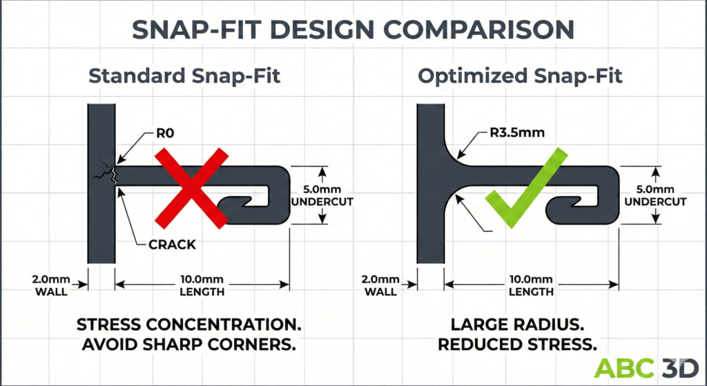
Conductive fillers, such as carbon nanotubes or carbon fiber, significantly alter the mechanical properties of the base polymer. While they add strength, they also increase stiffness and reduce elongation at break.
This means a standard 90-degree snap-fit designed for ABS might snap off when printed in Conductive ABS. To fix this, you should:
- Add Fillets: Remove all sharp internal corners. Use generous radii to distribute stress.
- Use “Lush” Curves: Design snap arms that taper gradually rather than abruptly.
- Avoid Living Hinges: Conductive materials are generally too stiff for flexible hinges; use mechanical hinges instead.
Orientation and Anisotropy
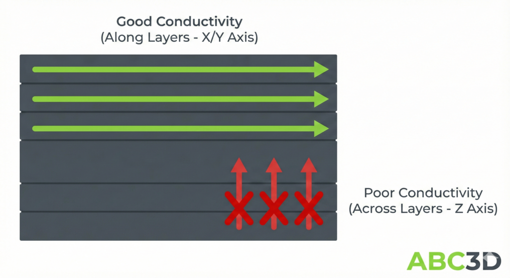
3D printed parts are anisotropic, meaning their properties vary depending on the direction. This is especially true for conductivity. Electricity flows much easier along the continuous strand of filament (X/Y axis) than it does hopping between layers (Z axis).
When orienting your part in the slicer, try to align the primary electrical path with the X/Y plane. If your current needs to travel vertically through the part, consider designing a channel for a metal pin or wire to bridge the layers.
Hardware Integration
Because conductive polymers are abrasive and stiff, self-tapping screws can cause cracking. For robust assembly, we strongly recommend using heat-set inserts. The brass insert not only provides a strong mechanical thread but also ensures an excellent electrical contact point for grounding wires.
By following these guidelines when designing for conductive 3D printing, you can transition from simple prototypes to production-grade electronic fixtures with confidence.
About ABC3D
ABC3D is a Canadian manufacturer of High-Performance & Conductive Polymers. We specialize in functional materials designed for the electronics, automotive, and aerospace sectors. Additionally, we bridge the gap between industrial-grade conductivity and environmental consciousness. Our team engineers materials for industrial applications, large-format printing, and injection molding.
For technical support or material inquiries, please contact:
Nivedita Narayan
Director of Products
info@abc3d.ca