
n the world of electronics manufacturing, precision and efficiency are paramount. The ability to prototype and produce custom circuit boards (PCBs) quickly is a game-changer for industries ranging from consumer electronics to industrial automation. Traditionally, PCB fabrication involves multiple steps, chemical etching, and expensive materials, making the process costly and time-consuming. However, 3D printing with conductive filaments is transforming PCB production, allowing manufacturers to print functional circuit boards on demand.
At ABC3D, we provide high-performance conductive filaments specifically designed for PCB prototyping and industrial electronics applications. Our materials offer an efficient alternative to traditional circuit board manufacturing, reducing development time and costs while enabling customized, low-volume production.
How 3D-Printed PCBs Are Changing Electronics Manufacturing
Printed circuit boards (PCBs) are the foundation of modern electronics, providing the electrical pathways that connect components. Typically, manufacturing a PCB involves complex chemical processes, multi-layer laminations, and precise machining, making it difficult and expensive for rapid prototyping.
With 3D printing and conductive filaments, manufacturers can now print PCBs in a single step, integrating both substrate (insulating base) and conductive traces in one process. This eliminates the need for chemical etching, simplifies design iterations, and allows for the creation of customized, application-specific circuit boards that would otherwise require outsourced fabrication.
Key advantages of 3D-printed PCBs include:
- Faster Prototyping – Engineers can quickly test and refine circuit designs without waiting for outsourced PCB production.
- Lower Production Costs – Eliminates expensive materials, chemical etching, and multi-step assembly processes.
- Custom Designs & Flexibility – Enables the creation of non-traditional PCB shapes, embedded circuits, and flexible electronics.
Optimizing PCB Printing with Conductive Filaments
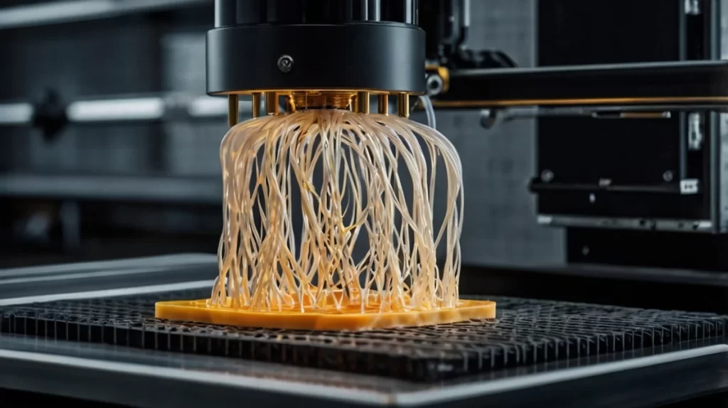
To achieve high-quality PCBs with 3D printing, it is essential to fine-tune printer settings, design parameters, and post-processing techniques. At ABC3D, our conductive filaments are optimized for maximum conductivity, adhesion, and durability, ensuring functional circuit pathways suitable for low-power applications, IoT devices, and sensor integration. When printing PCBs with conductive filaments, a few key factors must be considered. Printer calibration is essential for ensuring dimensional accuracy and electrical continuity. The print bed must be perfectly leveled to prevent gaps or misalignment in the circuit traces. Layer height and extrusion settings should be optimized to ensure consistent material flow and avoid breaks in conductivity.
Temperature settings also play a critical role. Conductive filaments often require higher extrusion temperatures (typically 220-250°C) to achieve strong inter-layer bonding, preventing circuit interruptions. Slower print speeds (around 30-40 mm/s) can enhance trace precision, reducing resistance and improving electrical flow.
For best results, circuit traces should be designed with wider paths to reduce resistance. Unlike traditional copper PCBs, 3D-printed conductive traces have higher resistivity, so increasing the width of the traces can significantly improve current flow and reliability.
Applications of 3D-Printed PCBs in Industrial Use
3D-printed PCBs are particularly beneficial for industries requiring custom, rapid, or low-volume circuit production. Some of the most promising applications include:
- IoT & Sensor Prototyping – Developers can create customized circuit boards for industrial IoT devices, testing different designs without the delays and costs of conventional PCB manufacturing.
- Wearable Electronics – Flexible conductive filaments, such as TPU-based materials, allow for the integration of bendable PCBs into wearable health monitors, smart textiles, and fitness devices.
- Aerospace & Automotive Applications – Lightweight, custom-shaped circuit boards can be designed for use in drones, electric vehicles, and avionics, optimizing space and weight while maintaining functionality.
- Education & Research – Universities and research labs can rapidly prototype functional PCBs, enabling experimentation with new sensor technologies, smart materials, and embedded systems.
Enhancing PCB Performance: Post-Processing Techniques
While 3D-printed conductive PCBs are highly effective for rapid prototyping, post-processing techniques can further enhance their electrical properties and durability.
One common approach is conductivity enhancement, where printed circuits are coated with conductive inks or electroplated to reduce resistance. This improves signal integrity, making the PCBs suitable for more complex applications. Additionally, conductive adhesives or low-temperature soldering can be used to connect electronic components to the printed traces, ensuring secure and long-lasting electrical contacts.
For multi-layer PCBs, techniques such as dual-extruder 3D printing can be used to combine conductive filaments with insulating materials, creating stacked circuit designs. This allows for more complex electronic layouts, bringing 3D-printed PCBs closer to traditional manufacturing standards.
Why ABC3D’s Conductive Filaments Are the Best Choice for PCB Prototyping
At ABC3D, we provide high-performance conductive filaments engineered for functional PCB prototyping and industrial electronics applications. Our materials are designed to offer:
- Superior Conductivity & Low Resistance: Optimized for efficient circuit pathways, reducing signal loss and improving electronic performance.
- Dimensional Accuracy & Layer Adhesion: Ensures precise circuit traces and strong inter-layer bonding for consistent electrical flow.
- Compatibility with Advanced 3D Printers: Works seamlessly with FDM and multi-material 3D printers, allowing for integrated PCB and device fabrication.
The Future of 3D-Printed Circuit Boards
As 3D printing technology continues to evolve, 3D-printed PCBs will become increasingly sophisticated and reliable. Advances in high-conductivity filaments, multi-material printing, and AI-driven circuit design will push the boundaries of what’s possible in on-demand electronics manufacturing. The integration of conductive polymers with smart materials may even lead to self-healing circuits and dynamic electronic components in the near future.
At ABC3D, we are committed to leading this transformation, providing manufacturers, researchers, and electronics developers with the best conductive filaments for next-generation PCB production. Whether you’re designing custom circuit boards for IoT, wearables, or industrial automation, our materials ensure fast, cost-effective, and high-performance results.
Get Started with 3D-Printed PCBs Today
With ABC3D’s conductive filaments, you can revolutionize your PCB prototyping process, eliminating traditional manufacturing constraints while unlocking new levels of design freedom and efficiency. Whether you’re a startup developing smart devices, an R&D team pushing electronics innovation, or an industrial manufacturer optimizing production, our filaments deliver the precision and conductivity you need.
Explore our range of conductive filaments today and bring your 3D-printed circuit boards to life! Need expert advice? Contact ABC3D’s team to optimize your designs and printing techniques for industrial PCB manufacturing.